Takayuki Ohba Laboratory,
WOW Alliance Heterogeneous and Functional Integration Unit,
Institute of Innovative Research, Science Tokyo
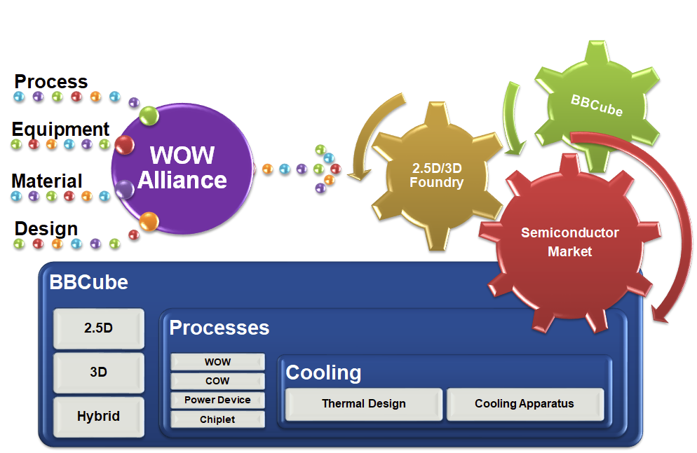
The WOW Alliance is an industry-academia R&D platform encompassing 3DI process technology, BBCubeTM design, thermal design, power transistors, supporting equipment, materials, analysis, and measurement. There are approximately 40 organizations and 160 researchers from companies and research institutions. WOW Alliance conducts project activities to optimize the BBCube system, coordinating each technology in line with practical application milestones. This is the only organization in Japan conducting practical application research and development using 300mm wafers.
The BBCube three-dimensional large-scale integration system being developed by the WOW Alliance can stack multiple layers of DRAM and CPUs until thinned to their physical limits. This results in the shortest possible vertical interconnect lengths (10µm) and ultra-parallel high-density connections. The transmission performance and power consumption of systems created with this technology are both world-leading, enabling high-density devices despite serious heat generation issues. In BBCube, the volume density of transistors increases in proportion to the number of layers stacked, making it a new semiconductor integration technology that bridges post-scaling and further miniaturization.
To address the reliability and productivity challenges of three-dimensional integration, we have developed a Via-Last TSV WOW/COW 300mm wafer process that does not use bumps or mechanical attachments for wiring connections. Via-Last TSV is a backward deployment of technology that has been verified for reliability in 10 trillion connections of BEOL 50nm vias, making it highly compatible with mass production. This technology can also be applied similarly to chiplets using Waffle wafers in COW.
Research Unit Leader Takayuki Ohba

Takayuki Ohba Profile
2013 Tokyo Institute of Technology, Professor
2004 The University of Tokyo, Professor
1984 Fujitsu Limited
National Chiao Tung University (NCTU Taiwan)
Visiting Professor
Ph.D received from Tohoku University in 1995
Tokyo Tech WOW Alliance
3-micronmeter Ultra-Thinnig 300mm SDRAM


2024/5/27
Our research was published in the Newspaper by the Nikkan Kogyo Shimbun, Ltd.
2023/6/29
Published in Tokyo Tech News [Implementing CPU/GPU and Memory in a Hybrid 3D Approach]
2022/10/26-10/28
A. Myalitsin received ”Packaging–Best Paper Award” by IMPACT 2022 (17th International Microsystems, Packaging, Assembly and Circuits Technology Conference). [Article]
2022/10/26
Published in Tokyo Tech News [Tokyo Tech WOW Alliance and NCKU Agree on Technical Partnership for 3D Integrated Technology based on BBCube]
2021/6/22
Published in Tokyo Tech News [No Space Wasted: Embedding Capacitors into Interposers to Increase Miniaturization]
2021/6/1-6/4
Z-W. Chen received ”Outstanding Session Paper” by 2021 IEEE 71st Electronic Components and Technology Conference (ECTC). [Article]
2021/3/21-3/24
Z-W. Chen received ” 2021 program highlighted papers” by 2021 IEEE International Reliability Physics Symposium (IRPS) . [Article]
2020/6/22
Published in Tokyo Tech News [Achieves stealth dicing without damaging the wafer]
2020/2/10
Three-dimensional stacking technology was published on the cover and magazine of the bulletin "Applied Physics Vol. 89, No. 2 (2020)". [Magazine]
2017/4/26
Published in Tokyo Tech News [Thermal resistance has been reduced to 1/3 with 3D DRAM of WOW technology]
2015/11/18
The closed-type plant ecology measurement device "SRP-450" jointly developed by Ohba Laboratory, Asahi Kogyo Co., Ltd., and TAZMO CO.,LTD. was introduced on Nikkei Technology Online.
[Article] [SRP-450 Pamphlet ]
2014/6/9
Published in Tokyo Tech News [300mmウエハーを厚さ4マイクロメートルに超薄化]
Three-Dimensional Integration Process Technology
We will use the ultra-thinning technology and the vertical interconnect technology possessed by the WOW Alliance to integrate semiconductors three-dimensionally and create a next-generation semiconductor that is higher in performance and lower in power consumption. Furthermore, this work will accelerate the ultra-miniaturization of not only large-scale computing devices such as servers, but various devices equipped with semiconductors to 1/1000th of their current size.
Three-Dimensional Integration Design and Architecture
We propose 3DI architecture and design technology that make use of BBCube's excellent electrical and thermal characteristics such as low capacitance, low inductance, and low thermal resistance, and accelerate high performance, low power consumption, and miniaturization in a wide range of devices, from HPC/AI to sensor-integrated edge devices.
Three-Dimensional Integration Cooling Technology
By combining ultra-small cooling devices with three-dimensional stacked semiconductors, our work will allow for simplification of cooling technology and application to the miniaturization of IoT and mobile devices.
Wide Band Gap Semiconductor
Aiming to promote green innovation using wide band gap power devices, from the perspective of material science to system device application.
Specifically, focusing on low-cost epitaxial technology and thermal management technology, the goal is to develop them into 3D-integration technology.